23

Feb . 2022

SiC device design philosophy – overcoming the challenges

Share to

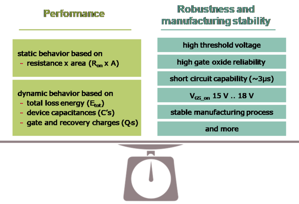
Figure 1: Robustness and manufacturing stability (right) of a SiC MOSFET have to be balanced with performance parameters (left)

The performance potential of silicon carbide (SiC) is undisputable, but designers have to master a key challenge: to determine which design approach achieves the biggest success in their application. But what are the strategies?


Advanced design activities are focusing on the field of a specific on-resistance as the major benchmark parameter for a given technology. However, it is essential for engineers to find the right balance between the primary performance indicators like resistance and switching losses, and the additional aspects relevant for real-world power electronics developments, for example sufficient reliability.


A suitable device concept should allow a certain design freedom in order to adapt to the needs of various mission profiles without significant changes in processes and layout. However, the key performance indicator will still be a low area-specific resistance of a chosen device concept, ideally in combination with the other listed parameters. Figure 1 shows a few criteria that we consider as essential, and we could add more.

Figure 2: Sketch of a planar DMOS SiC MOSFET (left), and a vertical trench TMOS SiC MOSFET, and the corresponding locations of resistance-relevant contributions

One of the most important acceptance criteria is the reliability of a component under the operating conditions of its target application. The major difference to the established silicon (Si) device world is the fact that SiC components operate at much stronger internal electric fields. So, designers should analyze the related mechanisms with great care. What Si and SiC devices have in common is that the absolute resistance of a part is defined by the series connection of contact resistances at drain and source.


This includes the highly doped areas close to the contact, the channel resistance, the resistance of the JFET (Junction Field-Effect Transistor) area, and the drift zone resistance (see figure 2). Please note that in high-voltage silicon MOSFETs (Metal-Oxide-Semiconductor Field-Effect Transistors), the drift zone clearly dominates the total resistance. In silicon carbide devices, engineers can design the drift zone in the device with a significantly higher conductivity as stated above.


Figure 3: Left: Typical structure of a planar MOSFET (half-cell). It reveals two sensitive areas with respect to oxide field stress.

Figure 3: Right: Typical structure of a trench MOSFET (half- cell). The critical issue here is the oxide field stress at the trench’s corners.

Regarding the key MOSFET element, the interface between silicon carbide and silicon dioxide, designers have to consider the following differences compared to silicon:


  • SiC has a higher surface density of atoms per unit area as silicon, resulting in a higher density of dangling Si- and C-bonds. Defects in the gate oxide layer near the interface may energetically appear within the energy gap, and act as traps for electrons [1].
  • The thickness of thermally grown oxides strongly depends on the crystal plane.
  • SiC devices operate at much higher drain-induced electric fields in the blocking mode compared to their Si counterparts (MV instead of kV). This requires measures to limit the electric field in the gate oxide to maintain the reliability of the oxide in blocking stage [2]. See also figure 3: for TMOS (Trench MOSFET), the critical point is the trench corner, and for DMOS (Double-Diffused Metal-Oxide-Semiconductor), it is the center of a cell.
  • SiC MOS structures show for a given electric field a higher Fowler-Nordheim current injection compared to Si devices because of a smaller barrier height. Consequently, engineers have to limit the electric field on the SiC side of the interface [3, 4].

The interface defects mentioned above result in a very low channel mobility. Therefore, they cause a high contribution of the channel to the total on-resistance. Thus, the advantage of SiC versus silicon in the form of a very low drift zone resistance is diminished because of the high channel contribution.


Keeping the oxide field stress under control


An observed way to overcome this dilemma is to increase the electric field applied across the oxide in on-state, either through a higher gate source (VGS(on)) bias for turn-on or by comparably thin gate oxides. The applied electric fields exceed the values typically used in silicon-based MOSFET devices (4 to 5 MV/cm vs. 3 MV/cm max. in silicon). Such high fields in the oxide in the on-state can potentially accelerate wear and limit the capability of screening remaining extrinsic oxide defects [1].


Figure 4: Sketch of the CoolSiC™ MOSFET cell structure

Based on these considerations, it is clear that planar MOSFET devices in SiC actually have two sensitive areas with respect to oxide field stress, as shown in the left part of figure 3. First, the discussed stress in reverse mode in the highest electric field area close to the interface between drift region and gate oxide. And secondly, the overlap between gate and source which is stressed in on-state.


A high electric field in on-state is considered as being more dangerous, since no device design measures are in place which could reduce the field stress during on-state as long as the on-resistance performance has to be guaranteed. Our overall goal is to combine the low RDS(on) offered by SiC with a working mode in which the part operates in the well-known safe oxide field-strength conditions.


Hence, we decided to forgo the DMOS technology and to focus on trench-based devices from the beginning. Moving away from the planar surface with its high-defect density towards other more favorable surface orientations enables a low channel resistance at low oxide fields. These boundary conditions are the baseline for applying quality assurance methodologies established in the silicon power semiconductor world in order to guarantee the FIT (Failure in Time) rates industrial and automotive applications expect.


We developed the CoolSiC™ MOSFET cell design to limit the electric field in the gate oxide in on-state as well as in off-state (see figure 4). At the same time, it provides an attractive specific on-resistance for the 1200 V class, which is achievable even in mass production in a stable and reproducible way. The low on-resistance allows for low VGS(on) voltage levels of only 15 V, together with a sufficiently high gate-source-threshold voltage of 4.5 V typically. These values are benchmarks in the landscape of SiC transistors.


Special features of the design include the orientation of the channel at a single crystallographic orientation via a self-aligning process. This ensures the highest channel mobility and narrows the threshold voltage distributions. Another feature are the deep p-trenches intersecting the actual MOS trench in the center in order to allow narrow p+ to p+ pitch sizes for effective screening of the lower oxide corner.


In summary, we can say that the design philosophy applied to our CoolSiC™ devices provided not only a good on-resistance but also reliable manufacturing process for mass production.


References


[1] Z. Chbili, A. Matsuda, J.Chbili, J.T. Ryan, J.P. Campbell, M. Lahbabi, D.E. Ioannou, and K.P. Cheung.: Modeling Early Breakdown Failures of Gate Oxide in SiC Power MOSFETs, IEEE Trans. Electr. Dev., Vol. 63, No. 9, pp. 3605–3613, 2016

[2] J. Lutz, T. Aichinger and R. Rupp.: Reliability Evaluation, in K. Suganuma (Ed.): Wide Bandgap Power Semiconductor Packaging: Materials, Components, and Reliability, Elsevier, 2018

[3] R. Singh, and A.R. Hefner.: Reliability of SiC MOS devices, Solid-State Electronics, Vol. 48, pp. 1717-1720, 2004

[4] K. Matocha.: Challenges in SiC power MOSFET design, Solid-State Electronics, Vol. 52, pp. 1631–1635, 2008

Semiconductor Components Inquiry Form
If you have any questions related to our products (qutation, technical support, product documents, sample request, cooperation, etc), please kindly fill the inquiry form. Your inquries will be replied as soon as possible.
Privacy Policy

STEP

01
!

Marked Please fill in the required field, thank you.

Need
Industry

Product

Notes

Next, fill in contact information

STEP

02
!

Marked Please fill in the required field, thank you.

Company Name
Department
Contact Person
Title
Phone number
eMail
Address
Delivery Address
Trading company or not
Verification Code
Subscribe to Newsletter
!

Marked * Please fill in the required field, thank you.

Company Name
Department
Name
Title
Contact Number
Select preferred newsletter language
Email
Verification Code